日立とインテル、製造業向けのフィジカルAI協業を発表
日立とインテル、製造業向けのフィジカルAI協業を発表
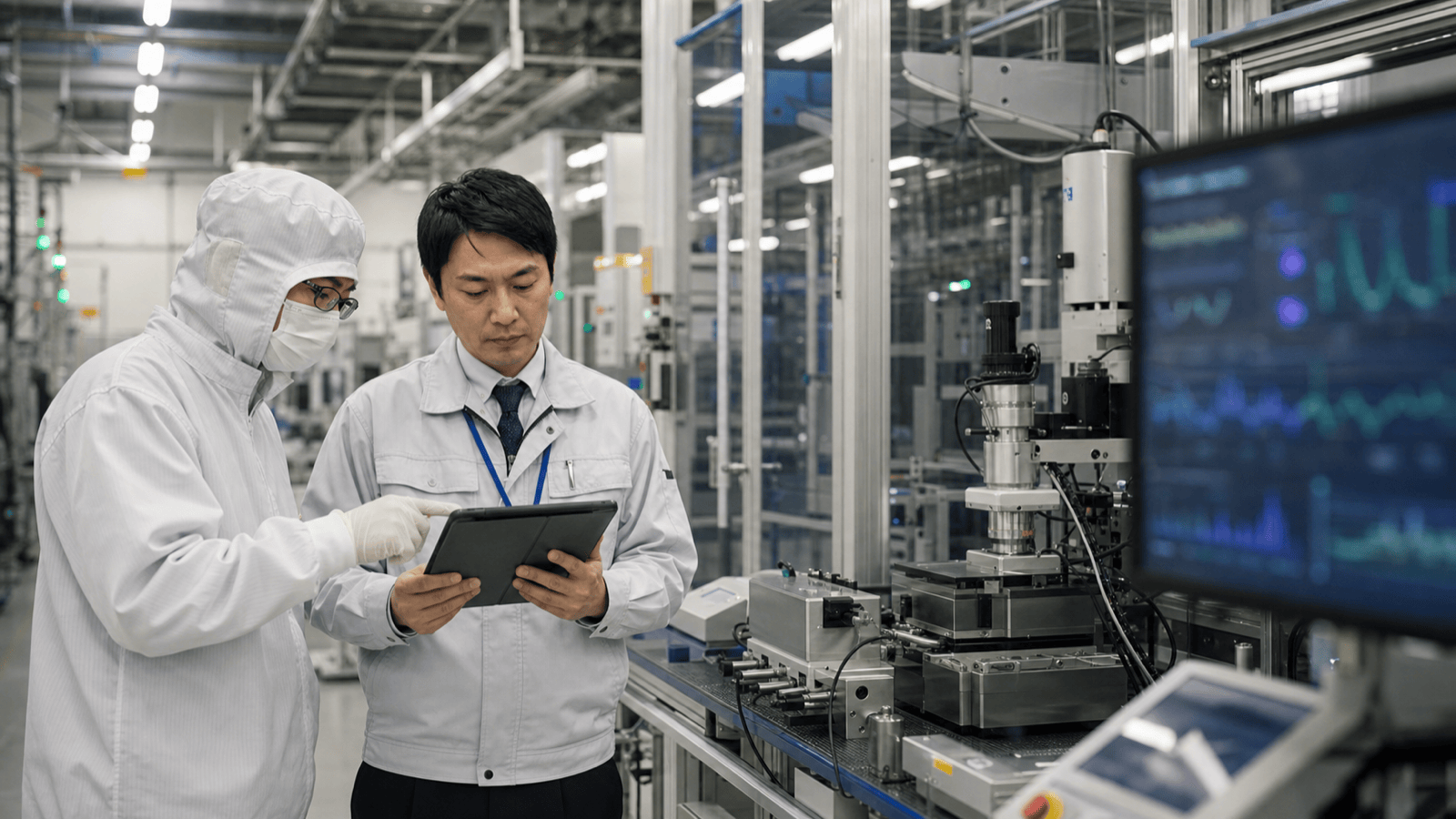
日立製作所は6月5日、インテルとの戦略的協業を広げると発表した。対象はフィジカルAIで、製造、エネルギー、モビリティの現場で使うシステムが中心だ。
Hitachi said on June 5 that it will broaden its strategic collaboration with Intel. The focus is physical AI, centered on systems used in manufacturing, energy, and mobility settings.
発表文によると、日立のOTとLumadaを、インテルのエッジAI、専用シリコン、半導体製造の知見と組み合わせる。産業データを集めるだけでなく、現場判断まで短くすることが狙いとされた。
According to the release, Hitachi's OT and Lumada will be combined with Intel's edge AI, custom silicon, and semiconductor process expertise. The aim is not only to collect industrial data but to shorten the path to on-site decisions.
フィジカルAIをどう使うのか
日立はフィジカルAIを、産業用アセットとデジタル制御を結び付ける 考え方として説明した。設備の状態を読み取り、その結果を運転や保守に返す 流れを強める 構想だ。
Hitachi described physical AI as a way to connect industrial assets with digital control. The concept is to read equipment conditions and feed those results back into operations and maintenance.
具体例としては、映像やセンサーから異常を見つけるエッジAI、工場の電力消費を調整する制御、移動体の安全運行などが挙げられた。つまりAIモデルだけでなく、動く 機械や電力網まで含める 話になっている。
Examples included edge AI that detects anomalies from video and sensors, control systems that tune factory power consumption, and safe operation of moving assets. In other words, the story extends beyond models into machines and power networks.
半導体でも協力
両社は半導体の分野でも協力を深める。日立ハイテクのCD-SEMと計測技術を、インテルの先端工程で使うと説明した。エッチング装置の診断や歩留まりの改善にも広がるとされた。
The two companies also plan deeper cooperation in semiconductors. Hitachi said Hitachi High-Tech's CD-SEM and metrology technologies will be used in Intel's advanced processes, expanding into etching-tool diagnostics and yield improvement.
ここはソフトウェア読者にも重要だ。半導体製造では、検査データ、装置ログ、工程ごとの差を連続的に扱う。運用技術とAIが結び付くと、分析だけでなく制御まで近づく。
This matters to software readers too. Semiconductor manufacturing continuously handles inspection data, equipment logs, and process variation, so bringing OT and AI together moves the stack closer not just to analysis but to control.
電力とチップ設計の接点
発表では、日立のHMAX Energyにインテルの技術を組み込み、ファブの電力管理を最適化するとした。高電圧シリコンを使う 電源 装置も共同開発するという。
The release also said Intel technology will be embedded into Hitachi's HMAX Energy to optimize fab power management. The companies also plan joint work on high-voltage silicon-based power devices.
AI需要でデータセンターとファブの電力負荷が増えるなか、消費電力をどう下げるかは経営だけでなく設計の課題でもある。日立とインテルは、その問題を電源とチップの両面から解く 構えを示した。
As AI demand increases power load in data centers and fabs, reducing electricity use has become a design issue as much as a management issue. Hitachi and Intel are presenting a two-sided response through both power systems and chips.
量子と移動体まで広げる
両社はさらに、量子コンピューティングや鉄道、車両、そのほかの移動体にも協力を広げるとした。現場データを扱う 基盤が共通化すれば、別々だった案件を横断できる可能性がある。
The partners also said they will extend cooperation into quantum computing, rail, vehicles, and other mobility systems. If the underlying data platform becomes more common, projects that used to stay separate may be handled across domains.
ただし、今回の発表は設計図に近い 段階でもある。売上 規模や納入時期はまだ細かく 示されていない。そのため、どの領域で先に実装が進むかは今後の説明が必要とみられる。
At the same time, this announcement is still close to a blueprint stage. Revenue scale and delivery timing were not detailed, so further explanation will likely be needed on which domains move into implementation first.
日本発の産業AIとしての意味
最近のAI報道はチャットや検索に偏りがちだが、今回は工場、電力、半導体という重い 産業を一つの話にまとめた点が特徴だ。日本企業のOTと、インテルの計算資源や製造技術を束ねる 構図になっている。
Recent AI coverage often leans toward chatbots and search, but this announcement stands out by tying factories, power systems, and semiconductors into one story. It bundles a Japanese company's OT with Intel's compute and manufacturing technology.
読者がソフトウェアやインフラのエンジニアなら、この協業はAIモデルそのものより、データ収集、エッジ推論、電力最適化、専用シリコンをどう一枚の運用に載せるかという課題として読むと分かりやすい。その統合力が、これからの産業AIで差になるとみられる。
For software and infrastructure engineers, the more useful way to read this collaboration is not as a model story but as a systems story about combining data collection, edge inference, power optimization, and custom silicon into one operating layer. That integration capability appears likely to become a differentiator in industrial AI.