ニコン、先端パッケージ向け1.5μm露光装置を開発
ニコン、先端パッケージ向け1.5μm露光装置を開発
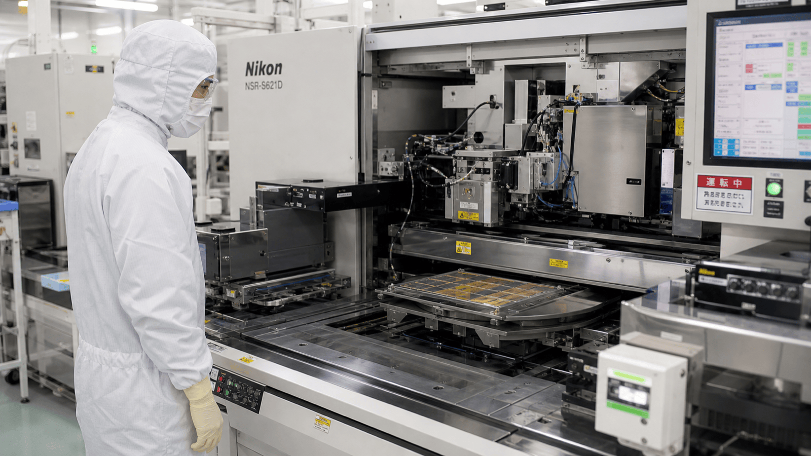
ニコンは6月5日、半導体の後工程で使う 先端パッケージ向けのデジタル露光装置を開発中だと発表した。1.5μmの解像度に対応しながら、処理速度も高める 狙いだ。
On June 5, Nikon said it is developing a digital lithography system for advanced packaging in semiconductor back-end production. The aim is to support 1.5 micrometer resolution while also raising throughput.
同社は、現在のDSP-100が達成する1時間あたり50パネルから、65パネル以上へ引き上げることを目標にしている。これは30%超の生産性 向上に当たる。
Nikon says it is targeting 65 panels per hour or more, up from 50 panels per hour on the current DSP-100. That would amount to more than a 30 percent productivity gain.
後工程が重くなる理由
生成AIの普及で、GPUやHBMのような次世代 半導体の需要が伸びている。その結果、複数のチップをつなぐ 先端パッケージの重要性も上がっている。
As generative AI spreads, demand is growing for next-generation chips such as GPUs and HBM. As a result, advanced packaging that connects multiple chips is becoming more important.
特に、大きいインターポーザーやFC-BGA基板では、細かい 配線をどう量産するかが課題になる。用途ごとに必要な解像度が違うため、最小化だけでなく処理量との両立が求められる。
Large interposers and FC-BGA substrates especially raise the question of how to mass-produce fine wiring. Because required resolution differs by use case, manufacturers have to balance small features with usable throughput.
ニコンが作るもの
新しい 装置は1.5μmの解像度に最適化した光学系を載せる 設計で、2027年度の発売が予定されている。より高い 生産性を優先した位置付けといえそうだ。
The new tool is designed around optics optimized for 1.5 micrometer resolution, and Nikon plans to release it in fiscal 2027. It appears to be positioned as a higher-productivity option.
一方で、光学系を交換すれば、DSP-100と同等の1.0μm解像度にも対応可能だという。顧客が将来のプロセス変更に合わせやすいようにした形だ。
At the same time, Nikon says the optical system can be swapped so the platform can also support 1.0 micrometer resolution like the DSP-100. That is meant to make future process changes easier for customers.
このデジタル露光装置はフォトマスクを使わない。マスク 製造コストを減らし、設計変更への対応を速めることで、試作から量産までの時間を短くする 効果が見込まれる。
This digital lithography system does not use photomasks. That can reduce mask-manufacturing costs and speed up response to design changes, shortening the path from prototyping to mass production.
日本の装置 戦略として
日本企業は、露光、材料、検査など個別の工程で強みを持つことが多い。先端パッケージは、その積み上げが生きる 分野だと見られる。
Japanese companies often have strengths in individual process steps such as lithography, materials, and inspection. Advanced packaging is seen as a field where that layered expertise can matter.
ニコンの発表は、解像度を少し 緩めてでも処理量を増やす 需要が確実にあることを示す。これは、AI向けチップの供給で後工程が制約になっている現状ともつながる。
Nikon's announcement suggests there is real demand for somewhat relaxed resolution if it comes with higher throughput. That lines up with the current reality that back-end packaging has become a supply constraint for AI-oriented chips.
発売は2027年度 予定なので、業績への反映はまだ先になる。それでも、日本の半導体 装置メーカーがどこで差別化するのかを考える 材料としては十分に興味深い 動きだ。
Because release is planned for fiscal 2027, the effect on business results is still some distance away. Even so, it is an informative move for thinking about where Japanese semiconductor-equipment makers may differentiate.